![]()
![]()
![]()
- HOME
- Product information
- Machine tools business
- Inspection and measuring machines


Inspection and measuring machines
Starting from semiconductor package AVI machines, we offer a lineup of various AVI machines for electronic and automotive components with good quality control. We provide optimal proposals based on consideration of the optical environment, with algorithm development according to your workpieces, using our extensive experience and expertise in 2D/3D measurements and various defect inspections.
Semiconductors/Electronic components
-
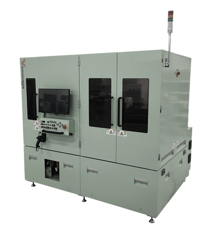
LI920S/LI900W
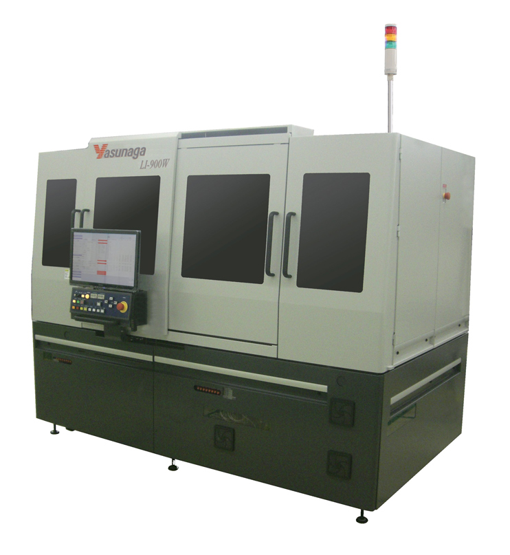
All-rounder in semiconductor IC package inspection
This is a tray-to-tray storage type AVI machine that supports a wide range of IC packages. Equipped with top surface, bottom surface, and terminal dimension inspection functions , it can also be equipped with optional functions for side surface inspection and foreign particle removal. It performs high-precision appearance inspection for in-vehicle ICs that require high quality control.
- Target workpieces: Surface mount IC packages (BGA, CSP, QFP, SOP, QFN, LGA, etc.), Image sensors, Sensors
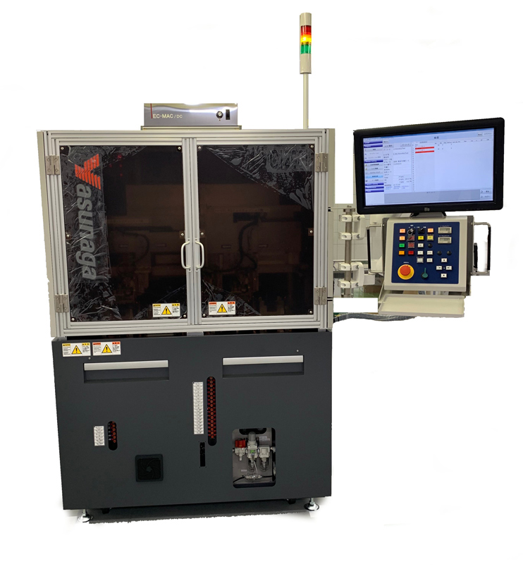
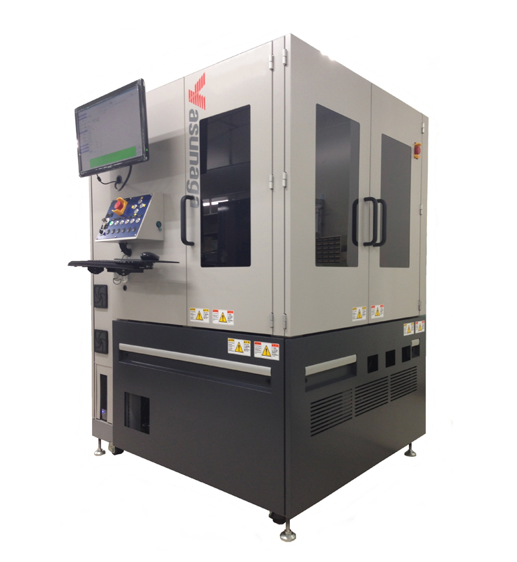
TIT1000Y/TIT2000Y
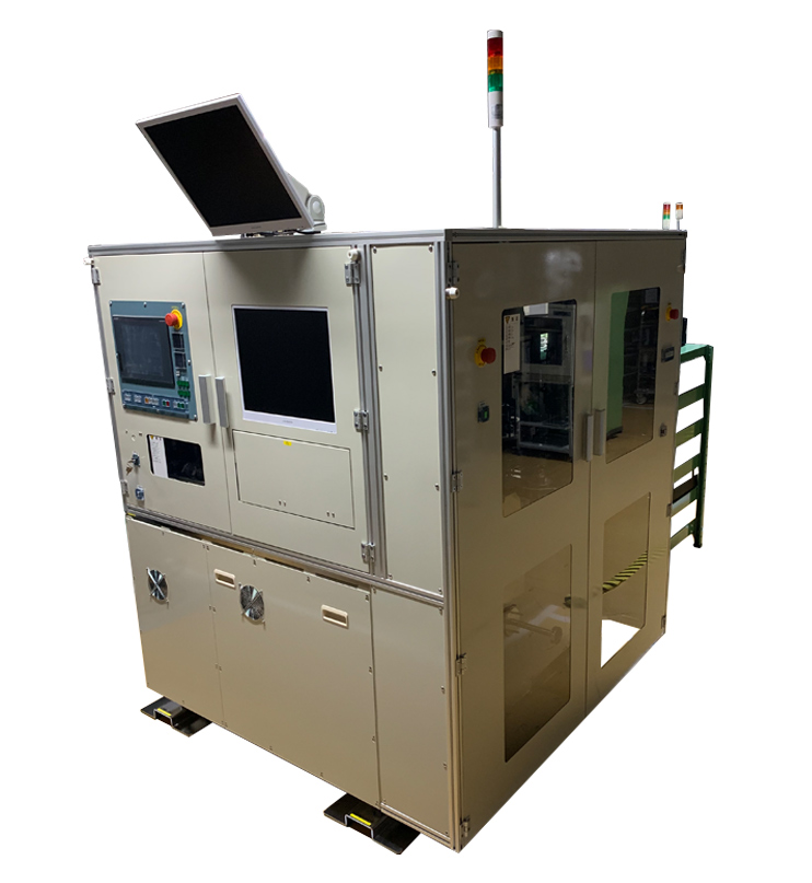
AVI machine capable of in-vehicle component quality inspections with embossed carrier tapes
This is a tray-to-taping storage type AVI machine that supports a wide range of IC packages. Equipped with top surface, bottom surface, and terminal dimension inspection functions, it also performs high-precision appearance inspection for in-vehicle ICs that require high quality control.
- Target workpieces: Surface mount IC packages (BGA, CSP, QFP, SOP, QFN, LGA, etc.)
LI700E
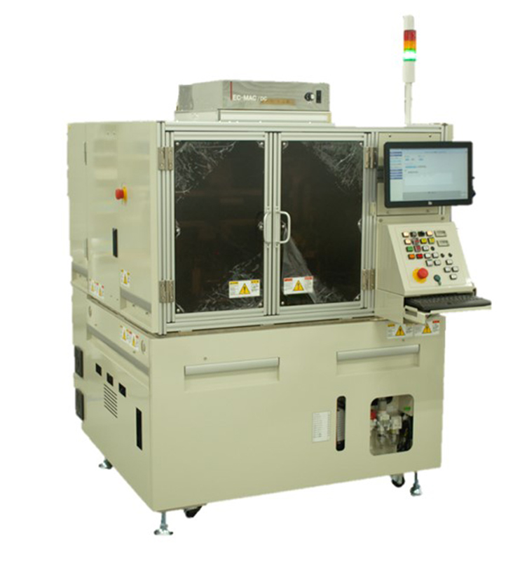
Compact and space-saving AVI machine for IC packages
This is a compact and space-saving AVI machine specialized for terminal dimension inspection of IC packages. It can be used for in-line or acceptance inspection, inspects pin bending, scratches, and damage which occur during ROM writing using the dimensional inspection and defect inspection functions to support quality control.
An optional surface inspection function is available.- Target workpieces: Surface mount IC packages (BGA, CSP, QFP, SOP, QFN, LGA, etc.)
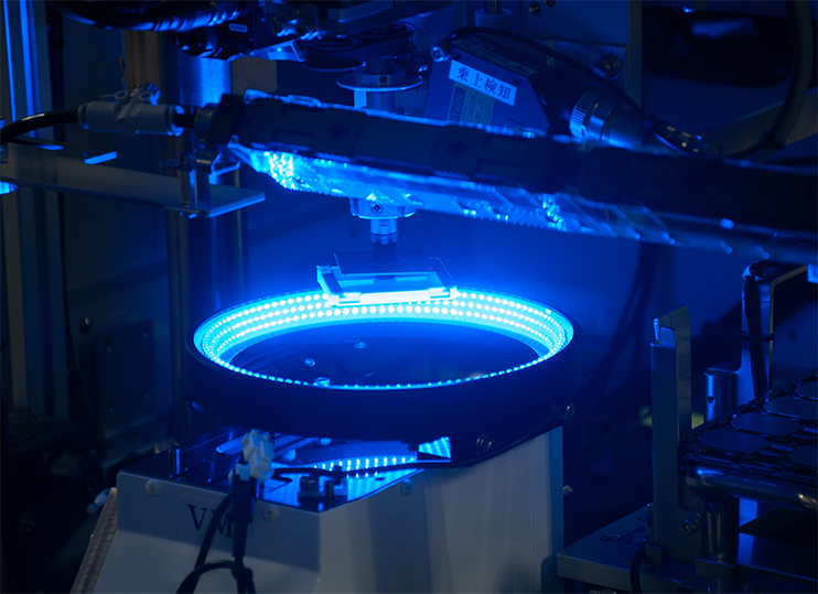
2D/3D inspection unit
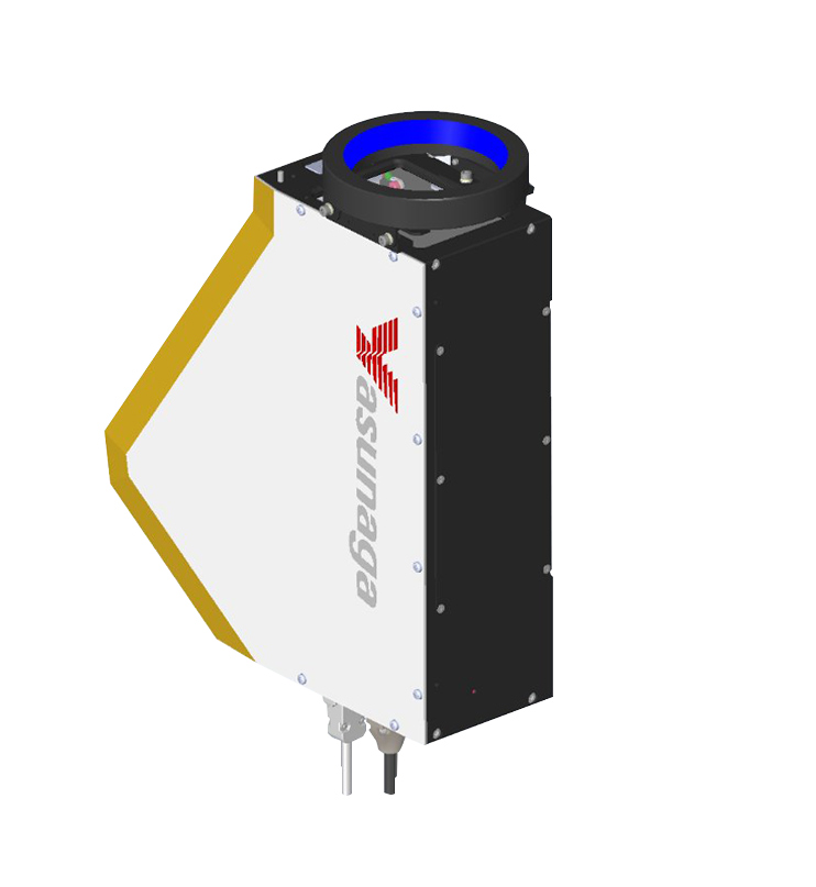
Highly precise inspection unit with 2D and 3D inspecting functions
This unit performs highly precise 2D/3D inspection at high speed in a single casing.
It supports a wide range of dimensional inspections, such as terminal dimension inspection of semiconductor IC packages, specified by JEITA standards, and 2D/3D component inspection.- Target workpieces: Surface mount IC packages, Chip components, Ceramic material parts We support a wide range of products.
Bare chips
-
CI8000
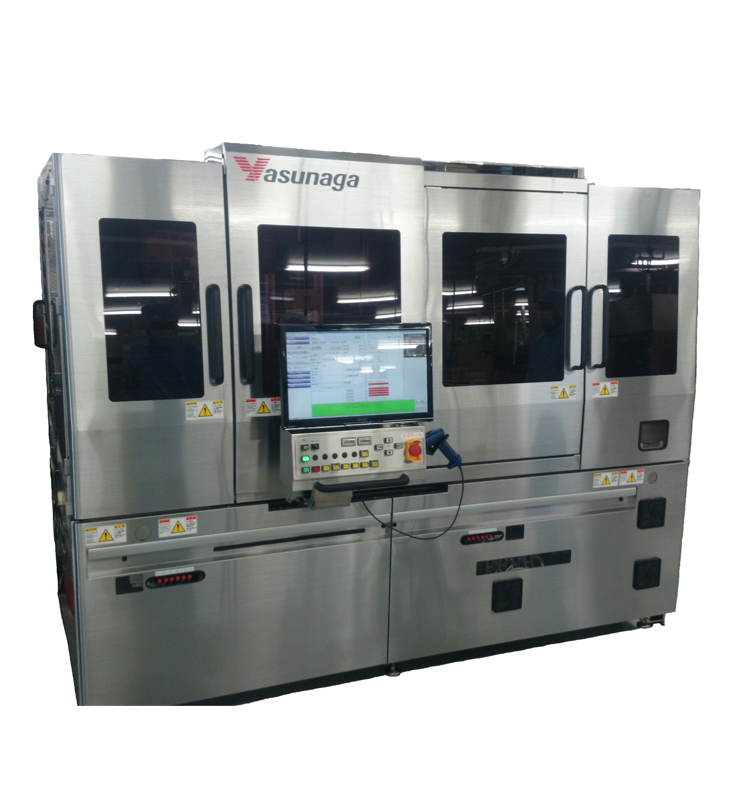
High throughput & 6-surface inspection for bare chips
This is a tray-to-tray storage type AVI machine that supports highly precise six-surface inspection of semiconductor bare chip components. Equipped with a highly precise stage to inspect top, bottom, and side surfaces, with high throughput of up to 8000 UPH.
- Target workpieces: Power semiconductor device, image sensor, optical communication device, etc.
CI200i
Space-saving, high-cost performance model for inspection on top and bottom surfaces of bare chips
This is a tray-to-tray storage type AVI machine that inspects semiconductor bare chip components with high accuracy. In-tray surface inspection is designed to save space and minimize damage caused by contact with the chips.
- Target workpieces: Power semiconductor device, Image sensor, Optical communication device, etc.
2D/3D inspection unit
Highly precise inspection unit with 2D and 3D inspecting functions
This unit performs highly precise 2D/3D inspection at high speed in a single casing.
It supports a wide range of dimensional inspections, such as terminal dimension inspection of semiconductor IC packages, specified by JEITA standards, and 2D/3D component inspection.- Target workpieces: Surface mount IC packages, Chip components, Ceramic material parts We support a wide range of products.
Ceramic substrate, Green sheet
-
FV53C
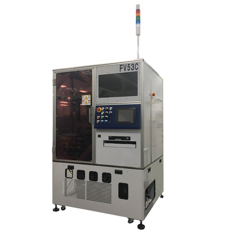
High speed inspection for wiring patterns of ceramic green sheets
This is an AVI machine for defect inspection of ceramic green sheets before the baking process.
Highly precise 3D inspection makes it capable of pattern inspection. Pattern position measurement can also be performed, in addition to defect inspection.- Target workpieces: Green sheets for multilayer ceramic components
FV203C
2D/3D inspection for ceramic substrates and other sintered substrates
This AVI machine supports top and bottom surface inspection for ceramic substrates.
In addition to defect appearance inspection, it can also inspect for slight bulges caused by internal expansion with its highly-precise 3D inspection function.- Target workpieces: Insulating ceramic substrates
2D/3D inspection unit
Highly precise inspection unit with 2D and 3D inspecting functions
This unit performs highly precise 2D/3D inspection at high speed in a single casing.
It supports a wide range of dimensional inspections, such as terminal dimension inspection of semiconductor IC packages, specified by JEITA standards, and 2D/3D component inspection.- Target workpieces: Surface mount IC packages, Chip components, Ceramic material parts We support a wide range of products.
Substrate, sheet
-
Customizable for appearance inspection of various substrates and sheet parts
This AVI machine supports highly precise inspection for substrates and sheet parts.
The broad lineup of models, including high resolution models and large FOV models, supports a wide variety of needs. This machine can also be customized for the front- and back-end transportation methods of the inspection process.- Target workpieces: Lead frame, Substrate, Module substrate
Other substrate products
- Target workpieces: Lead frame, Substrate, Module substrate
Magnetic materials
-
Centralized shipment management by combining 6-surface appearance inspection and weight measurement
This machine supports appearance inspection of the top, bottom, and side surfaces and weight measurement for magnetic products. The camera and lighting environment and loading/unloading sections can be customized according to the product size and shape.
- Target workpieces: Neodymium magnets, ferrite magnets, etc.
Motor, Battery
-
Customized AVI machine for electrification products such as motors and batteries
AVI machines can be specially designed for particular workpieces, such as motors, fuel cells, rechargeable batteries, and solar cells. An optimal inspection environment can be designed to perfectly suit the inspection target. Devices can also be customized according to the front- and back-end transportation methods of the inspection process.
Customization
We are capable of various customizations for transportation methods, inspection environments, and upper host in factories. We can support a wide range of customization levels, from semi-customization to full customization.
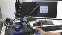
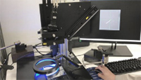
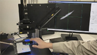
Sample test
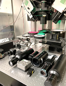
Various inspection target workpieces can be tested at AI GAKEN LABO.
We can propose optimal solutions, from consideration of the optical environment to development of dedicated algorithms according to your inspection target workpieces. Please feel free to contact us.
AI GAKEN LABO
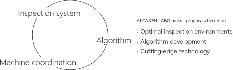
We have laboratories to test your actual workpieces. In the laboratories, the inspection environment is ready to support workpieces from various fields, including semiconductor, electronic, motor, battery-related, and machined components. We make overall proposals in terms of inspection environments and detection algorithm development based on the evaluation results.
By proposing solutions based on the inspection environment and equipment design, we can quickly support your automation needs.
 Wavelength
 Propagation
 Polarization characteristics
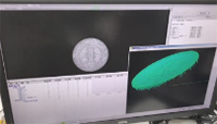 3D shape measurement
With two labs in the Head Office (Iga City, Mie Prefecture) and Tokyo Center, we can promptly test samples from customers.

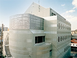
Head Office and Main Plant AI GAKEN LABO
Development and production of AVI machines
Experimental demonstrations and evaluation using AVI machines
3860 Midorigaoka Naka-machi, Iga City, Mie 518-0834, Japan
TEL: 81-595-24-2252 FAX: 81-595-24-2720
Yasunaga Tokyo Center AI GAKEN LABO
Research and development of appearance inspection units
Development of image processing inspection software
Experimental demonstrations and evaluation using appearance inspection units
3-4-1 Kamezawa, Sumida-ku, Tokyo 130-0014, Japan
TEL: 81-3-3621-3301 FAX: 81-3-3621-3828